B.Tech ECE - Semiconductor Design

Programme Overview

B.Tech ECE Specializing in Semiconductor Design is a newly created undergraduate course that addresses the growing requirements of the semiconductor business and microelectronics. It integrates the ideas of electronics and communications with knowledge in design, fabrication, and testing of semiconductor devices and systems.

This specialization is for gaining expertise in fields like Very-Large-Scale Integration (VLSI), nanoelectronics, chip design, fabrication processes, and electronic system-level design automation. This program supports India's Atmanirbhar Bharat policy and the worldwide shortage of semiconductors and has good career prospects both in the national and global markets.

Specializations Offered

  • B.Tech Electronics and Communication Engineering with specialization in Semiconductor Design.

Duration:  4 yrs. (8 Semesters)

Key Educational Benefit

Manav Rachna offers a unique educational experience that combines academic excellence, practical exposure, and industry partnerships to equip students with the skills needed for real-world success.

41,000+

Alumni Imprints Globally

2800+

Published Research Papers

600+

MNC's & Indian Corporate Recruit

250+

Patents (Filed/Granted)

120+

Global Academic Collaborations

80+

Alumni & In-Campus Startups

60+

Countries with Footprints

60 LPA

Highest CTC Offered

Eligibility

Minimum Eligibility Criteria

Pass 10+2 examination with a minimum of 55% marks in aggregate in the 5 below mentioned subjects:

  • English, Physics & Mathematics
  • Any one subject among the following list: Chemistry, Computer Science, Electronics, Information Technology, Biology, Informatics Practices, Biotechnology, Technical Vocational subject, Agriculture, Engineering Graphics, Business Studies, or Entrepreneurship
  • One subject on the basis of highest marks scored in the other subjects

*Note A: Chemistry / Computer Science/Electronics/Information Technology/Biology/Informatics Practices/Biotechnology/ Technical Vocational subject / Agriculture / Engineering Graphics / Business Studies / Entrepreneurship

Admission Criteria

Merit preparation and shortlisting of candidates will be based on XII Qualifying Examination marks, SAT, MRNAT, or JEE Mains.

Nationality

Home students of India and foreign students are eligible to apply.

  • Selection Criteria
  • Admission Criteria

Scholarship Programme - Utkarsh and Uttam

Merit scholarships for 100% fee waiver for merit achievers.

Programme Highlights

Industry-Specific Curriculum
Specific VLSI courses, CMOS design, device modeling, IC fabrication, and semiconductor physics.

Hands-On Learning with High-End Labs
Area for the most advanced labs for VLSI design, microelectronics, fabrication, and cleanroom process.

Association with Industry Leaders
Industry leadership collaboration and internship with industry giants such as Intel, TSMC, STMicroelectronics, and Texas Instruments.

Chip Design Tools & Software Focus
Teaching of the industry's best EDA tools such as Cadence, Synopsys, Mentor Graphics, and Xilinx Vivado.

Research-Oriented Approach
Freedom to work on subsidized semiconductor research projects and publish in conferences and journals.

Capstone Projects & Start-up Support
Year-long SoC design, ASIC/FPGA implementation, or fabrication-based projects with incubation support for entrepreneurial projects.

Fabrication & Testing Integrated Exposure
Hands-on exposure in lithography, doping, etching, packaging, and testing processes.

Semiconductor Domain Expertise Faculty
Classroom lectures by experienced faculty members with PhDs and industry backgrounds in semiconductor engineering.

Placement & Career Opportunities
Excellent placement record in semiconductor companies, EDA companies, defense R&D laboratories, and high-technology streams of education (MS/PhD).

Global Opportunities & Higher Education
Excellent foundation for graduate research in microelectronics, nanotechnology, and device physics in the universities of global excellence.

Internships with Semiconductor Companies
Opportunity in top companies such as Intel, AMD, Qualcomm, Texas Instruments, STMicroelectronics, NXP, and MediaTek, familiarizing students with real VLSI, chip design, testing, and fabrication.

Industrial Training Programs
Short training is conducted with design houses or fabrication labs and training centers for practical work using software like Cadence, Synopsys, Mentor Graphics, and Xilinx.

Industry-Sponsored Projects
Final-year or capstone project is undertaken in conjunction with actual semiconductor or EDA companies to solve real-world problems and are mentored by industry experts. Students have participated in theoretical workshops on RTL design, ASIC/FPGA implementation, or semiconductor physics presented by industry experts.

Industry Visits / Tours of Fabrication Labs
Students are taken to view the wafer fabrication process, cleanroom, and backend packaging through tours of a fabrication or research and development semiconductor centre.

Guest lectures / seminars from industry experts
Students are exposed to guest lectures by industry experts covering current trends in SoC design, AI chips, and low-power electronics, and in general career counselling and networking.

Hackathons, Design Competitions
Design competitions at local, national, and international levels, e.g., Cadence Design Contest and Intel FPGA Innovation Challenge offer students the opportunity for innovative circuit and system-level design creativity.

Industry-Led Curriculum / Co-teaching Modules
Created in partnership, or co-taught by industry professionals, the teaching package is continuously updated to reflect recent industrial needs.

Partnering with Semiconductor Startups / Incubators
Students gain experience prototyping, developing products and innovating in a startup environment with the possibility of IoT, wearables technology, or embedded chip solutions.

Professional Certification Programs
Industry tested certification through Coursera, etc.

Our Top Recruiters

Internship & Placement Opportunities

Internship

Industry-specific Internships: Internships give you exposure to real industry experience working with companies like Intel, Samsung Semiconductor, Qualcomm, Texas Instruments, NXP, and Cadence Design Systems.

Campus Internships: Work with faculty on short or longer term projects that deal with real world projects in VLSI, FPGA, MEMS, and embedded systems.

Government funded (Internships/Research opportunities): Summer internships and sponsored research project opportunities with ISRO, DRDO, MeitY and CDAC on chip design and nanoelectronics work.

Placement

Major recruiters: Intel, MediaTek, AMD, Synopsys, STMicroelectronics, Micron, TSMC India, and HCL Technologies.

Positions offered: VLSI design engineer, SoC verification engineer, Analog layout engineer, embedded systems developer and FPGA design engineer.

Placement readiness: Training was conducted in the following: Digital IC design, Analog IC design, Verilog, System Verilog, SPICE Model simulations tools and electronic design automation (EDA) tools from Cadence, Synopsys and Mentor Graphics.

Top Recruiters

  • Synopsys
  • Cadence
  • Mentor Graphics
  • FreeScale
  • Nokia
  • Vivo
  • Ericsson
  • Wipro Ltd
  • British Telecom
  • Evalueserve
  • TCS
  • IBM
  • Google
  • Capgemini
  • Coforge
  • Accenture
  • Expert Lancing Research
  • L&T Technology

At the forefront of India’s semiconductor mission, the B.Tech. in Electronics and Communication Engineering with a specialization in Semiconductor Design opens doors to cutting-edge career paths. The program is designed in collaboration with industry leaders to ensure graduates are prepared for the evolving needs of the semiconductor and EDA sectors.

Top Recruiting Sectors

Semiconductor Industry:

  • Chip companies (Intel, TSMC, Samsung)
  • EDA Dealers (Synopsys, Cadence, Mentor Graphics)
  • Electronics and Embedded Systems distributors (Texas Instruments, Qualcomm, STMicroelectronics)
  • Automotive electronics and transportation companies (NXP, Bosch, Infineon)
  • Telecommunication and 5G companies
  • Consumer electronics and IoT companies
  • Higher Education / Research Careers
  • Graduate students will be well prepared for
  • MTech/MS in VLSI design, embedded systems or microelectronics
  • PhD in semiconductor physics, nanoelectronics, and MEMS
  • Researcher at national lab or multi-national technology development company, or
  • Entrepreneurship (graduates may look at start-ups in)
  • Custom chip design, proof of concepts and prototyping Company from Re–Embedded product design and development
  • IoT hardware development and design

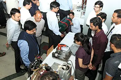
Capstone Project & Research

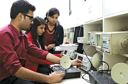
The Electronics and Communication Engineering (ECE) program at Manav Rachna integrates skill based events and workshops (e.g., LAM Semulator, Synopsys, Cadence software tools) to make sure that students leave the class room with a practical, hands-on experience. This practical learning experience enhances the experiential problem-based learning, the bridging of knowledge from theory to real-world thinking, as well as the aspects of innovation, understanding of technology, and problem-solving capabilities.

Capstone Projects require students to confront problems based on industry focused problems, and new and emerging technologies. Projects cover areas such as:

  • Embedded Systems & IoT
  • Wireless Communication Systems
  • Signal & Image processing
  • VLSI Design & Digital Systems

Faculty and students are engaged in research in the following thrust areas:

  • Artificial Intelligence & Machine Learning
  • Communication Systems
  • Sensor Networks & IoT Cyber Security
  • Biomedical Engineering

Innovation & Startups

Innovation and Startups are facilitated by the Manav Rachna Business Incubator, providing facilities, including;

  • Access to design, fabrication and manufacturing facilities
  • Research, innovation and entrepreneurship support
  • Access to capital from investors and government
  • Support from Investors, Network, Mentorship and expertise
  • Regulatory, finance and administrative support
  • Workshops, capacity building and training

Alumni Network

Alumni network, professionals working at organizations like Intel, Google, ISRO and creators/ artist like choreography and movie even!

It is a complete ecosystem in learning by doing, research, global exposure and access to support that equips ECE graduates at Manav Rachna University to pursue a diverse career path that has an impact in the world.

Global Exposure

Global Exposure occurs in limitless ways, including opportunities for global certifications, higher education and specialized training that every student can find a way to develop their career path globally.

Student Achievements

Student Achievements in Electronics and Communication Engineering (ECE):

  • National Winner, Microsoft Imagine Cup 2023: Mr. Anuvrat Kumar and Mr. Kartik Kachhawa achieved national recognition by winning this prestigious innovation competition.

Industry Placements and Internships:

  • Secured internship at Cadence in VLSI Design.
  • Ms. Boddu Alekhya and Mr. Pasupuleti Brahma Vishnu Vardhan received placement offers at Launched.
  • Abhishek Verma began an internship at Sadegel.
  • Mr. Yechuri Manjunadha was placed at Vivo.

Competitive Exam Success:

  • Mr. Mohammad Saad qualified the GATE 2025 Examination, demonstrating excellence in national-level engineering assessment.

Technical Event Awards at Innoskill 2025:

  • Mr. Manikanta, Mr. Dogga Hema Prasad, and Mr. Eshwar secured second position in the Annual Technical Event "Srijan."
  • Mr. Prashant, Mr. Rohit, Mr. Ashutosh, Mr. Ankur, and Mr. Sumit won first position in the "Vista Vibes" event.
  • Mr. Prashant Chauhan and Mr. Jay Deekshith achieved second position in "Vista Vibes."
  • Mr. Samarth Dhiman and Mr. Vansh Vishnoi secured first position in the "Build a Circuit" event.
  • Mr. T. Venkata Uma Mahesh, Mr. K. Eswar, Mr. Vignesh Karumuri, Mr. Surya Nikhil, and Mr. D. Charan secured second position in "Build a Circuit."

These achievements reflect the program’s strong industry orientation, emphasis on innovation, and student excellence in both technical and competitive domains.

Why Pursue ?

Electronics and Communication Engineering (ECE) is a branch of engineering that enables a vast number of opportunities due to being high-tech and having different cross-disciplinary applications across multiple high-growth sectors.

Faculty of ECE graduates may work in the electronics sector- in areas like chip design, embedded systems, and consumer electronics- as a design-in engineer on the development of advanced microchips and smart devices that collect and process information. The telecom sector is another area for ECE graduates that will consistently need skilled workers, as ECE graduates develop and maintain mobile networks, satellite communication systems, or internet infrastructure to facilitate wired and wireless devices. New surrounding technologies- like 5G and IoT- drive the demand for ECE graduates.

There are a diverse number of reasons that make ECE graduates attractive to other sectors, especially IT and software. There are many ECE graduates that become software developers, network engineers, or work in cloud support. Major IT companies are frequently hiring ECE graduates for their engineering, programming, and mathematical skills.

There are huge opportunities for the core PSUs at ISRO, DRDO, BEL, BSNL, etc., where graduates can work on national projects in defence, space, and communications. Also, skills in ECE have value in other industries such as automotive, aerospace, healthcare, medical devices, and energy and power; The agility of ECE is remarkable.

In case people are interested in pursuing higher studies, ECE provides a good platform to branch off into specific postgraduate multi-disciplinary programs, such as an M.Tech or MS programs related to, VLSI, robotics, signal processing, wireless communication, embedded systems, etc. It is also possible for graduates to pursue an MBA degree to become tech-managers and utilize both tech and management skills. Finally, research careers in India and abroad are quite plentiful and could help get them into academia or have opportunities to build cutting-edge products in the industry.

ECE is a multidimensional and evergreen discipline that allows graduates to follow any of a variety of technical, managerial, or research avenues. It places you at the cutting edge of innovation in such areas as AI, IoT, Robotics, and communication systems with skills that are applicable globally and are in high demand.

Fee Details for B.Tech ECE - Semiconductor Design

  • Course Level

    Course Fee (Annual): INR 2,20,300 US $ 3300

  • Duration

    Duration: 4 Years

  • MANAV RACHNA INTERNATIONAL Brochure (PDF)

Modes of Payment

  • Online Payment: Via net banking, debit/credit card, or UPI through the university's official payment portal.
  • Bank Transfer: NEFT/RTGS to the university’s designated bank account.
  • Demand Draft (DD): In favor of “Manav Rachna International Institute of Research and Studies”, payable at Faridabad/New Delhi
  • Cash Payment: At the Accounts Office on campus (subject to limits as per government regulations).
  • Education Loan: Through tie-ups with banks like PNB, SBI, HDFC, and ICICI, offering easy financing options.

Residential Facilities & Transport

We at Manav Rachna offer generous residential facilities and convenient transportation services so that each student, including those studying Manav Rachna, gets to enjoy a safe, comfortable, and fulfilling campus life.

Residential Services

MREI provides on-campus and off-campus hostel facilities for boys and girls with various types of rooms. Students can choose single, double, and triple rooms as per their preference.

Key Points

Room Types: The hostels offer different types of rooms to suit different budgets and preferences:

  • Air-conditioned and non-air-conditioned rooms
  • Single-seater, two-seater, three-seater, and five-seater rooms
  • The rooms can be equipped with attached or common toilets as per the choice of room category.

Fee Structure: The hostel fee is to be paid on the basis of the room category chosen by the student and it can be paid through DD (Demand Draft) or in cash.

Additional Facilities:

  • Medical services and medical insurance to keep the students fit.
  • Library facilities for access to study materials and academic inputs.
  • Laundry facilities as included in the hostel fees, to ease the life of students.

Mess Plan

At Manav Rachna, we offer world-class sports facilities to keep our students fit and active. Our facilities comprise a range of outdoor and indoor games, including:

Sports

Mess plan also comes as part of hostel fee. Healthy food is served through the mess considering the multicultural requirements of different food habits for the students. By providing choices involving vegetarian as well as non-vegetarian options, healthy lifestyle is available for the students enabling them to pursue their studies focusing on programs with full seriousness.

  • Basketball, volleyball, cricket, soccer, chess, and carom among others.

Notable facilities include:

  • A 25m shooting range and a 10m air-conditioned indoor shooting range with Olympic-standard SIUS Ascor electronic targets.
  • Indoor badminton and table tennis stadia with synthetic courts in association with Yonex and Stag.
  • A Semi-Olympic pool for swimming and a Soccer Academy for students who have sporting interest and passion.
  • A Sports Fitness Centre to service psychological, physiotherapy, and other aspects of health for students.

The facilities enable students to pursue physical exercises that complement their academic development.

Laundry

Laundry facilities are available at an extra fee in the hostel fees. This saves students from worrying about laundry, so they can focus on their studies, and also allows their clothes to remain properly cleaned.

Parking

There is a vast parking space facility available for students who commute using their own means of transport. It is provided to cater to the requirements of students, so that their travel will be easy and hassle-free.

Transport

Our well-maintained transport facility offers a stress-free, secure, and safe journey for students from Delhi and Gurugram. The GPS-located, contemporary fleet of buses is operated by professionally trained personnel, with onboard support staff to assist students. Our emphasis is on reliability, safety, and convenience, ensuring unproblematic travel to and from the campus.

How to Apply for B.Tech ECE - Semiconductor Design

Manav Rachna offers a unique educational experience that combines academic excellence, practical exposure, and industry partnerships to equip students with the skills needed for real-world success.

  • 1
    icon
    Go to the Official Website
  • 2
    icon
    Complete the Online Application Form
  • 3
    icon
    Upload Mandatory Documents
  • 4
    icon
    Pay the Application Fee
  • 5
    icon
    Appear for MRNAT or Submit JEE Score

Step 1 - Go to the Official Website

Log in to www.manavrachna.edu.in and click on the Admissions link.

Step 2 - Complete the Online Application Form

Click on "Apply Now," generate your login credentials, and fill out the form with your personal, educational, and contact information.

Step 3 - Upload Mandatory Documents

  • Upload scanned copies of the necessary documents, such as:
  • Class 10 & 12 mark sheets
  • Aadhaar card
  • Passport-size photos

Step 4 - Pay the Application Fee

Fill in the application by paying online using net banking, debit/credit card, or UPI.

Step 5 - Appear for MRNAT or Submit JEE Score

Get qualified through MRNAT (Manav Rachna National Aptitude Test) or produce a valid JEE Main score for merit-based admission.

PO's and PSO's

Program Outcomes (PO's)

PO1

Engineering knowledge

Apply the knowledge of mathematics, science, engineering fundamentals, and an engineering specialization to the solution of complex engineering problems.

PO2

Problem Analysis

Identify, formulate, review research literature, and analyze complex engineering problems reaching substantiated conclusions using first principles of mathematics, natural sciences, and engineering sciences.

PO3

Design/Development of Solutions

Design solutions for complex engineering problems and design system components or processes that meet the specified needs with appropriate consideration for the public health and safety, and the cultural, societal, and environmental considerations.

PO4

Conduct Investigations of Complex Problems

Use research-based knowledge and research methods including design of experiments, analysis and interpretation of data, and synthesis of the information to provide valid conclusions.

PO5

Modern Tool Usage

Create, select, and apply appropriate techniques, resources, and modern engineering and IT tools including prediction and modeling to complex engineering activities with an understanding of the limitations.

PO6

The Engineer and Society

Apply reasoning informed by the contextual knowledge to assess societal, health, safety, legal and cultural issues and the consequent responsibilities relevant to the professional engineering practice.

PO7

Environment and Sustainability

Understand the impact of the professional engineering solutions in societal and environmental contexts, and demonstrate the knowledge of, and need for sustainable development.

PO8

Ethics

Apply ethical principles and commit to professional ethics and responsibilities and norms of the engineering practice.

PO9

Individual and Team Work

Function effectively as an individual, and as a member or leader in diverse teams, and in multidisciplinary settings.

PO10

Communication

Communicate effectively on complex engineering activities with the engineering community and with society at large, such as, being able to comprehend and write effective reports and design documentation, make effective presentations, and give and receive clear instructions.

PO11

Project Management and Finance

Demonstrate knowledge and understanding of the engineering and management principles and apply these to one’s own work, as a member and leader in a team, to manage projects and in multidisciplinary environments.

PO12

Life-long Learning

Recognize the need for and have the preparation and ability to engage in independent and life-long learning in the broadest context of technological change.

Program Specific Outcomes (PSO's) 

Connect learning from Core and Disciplinary/Interdisciplinary elective courses of Electronics and Communication Engineering to assimilate technological advancements in the field for analyzing and designing subsystem processes to arrive at the solution to real world problems.

Acquire hardware and software skills pertinent to research and industry practices in the field of Electronics & Communications while acquiring soft skills like persistence, proper judgment through projects and industrial interactions.

Ability to identify indigenous processes and components for producing high quality, compact, energy efficient and eco-friendly solutions at affordable prices for existing and new applications directly and indirectly related to the Electronics & Communication industry

Focus on acquiring right blend of aptitude and attitude so as to be the candidate of first choice for placements and higher education or to become a successful Entrepreneur and a worthy global citizen.

Frequently Ask Questions

What is B.Tech ECE with specialisation in Semiconductor Design?

What are the eligibility criteria for admission to this programme?

Which core subjects are covered under the Semiconductor Design specialisation?

What are the career opportunities in the semiconductor industry after this course?

Does the curriculum include hands-on training in chip design and manufacturing?

Are there any industry partnerships or collaborations for this specialisation?

What software tools or platforms are taught for semiconductor design?

How is this specialisation different from a regular B.Tech in ECE?

Are internship or research opportunities available in the semiconductor field?

What is the future scope of Semiconductor Design in India and globally?

Contact Us

Icon location ADDRESS

Sector – 43, Aravalli Hills, Delhi – Surajkund Road, Faridabad – 121004, (Haryana), India